Foreløbige abstracts
Hent det foreløbige program (121 KB) - Updateret!
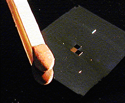
- Photonic crystal fibers infiltrated with liquid crystals
- theory and experiment
Jesper Lægsgaard and T. T. Alkeskjold, Technical University of Denmark - Plastiksolcelle forskning på Risø
Frederik Krebs, Research Center Risø - Laser Micromachining at the Danish Technological Institute
Martin F. Jensen, Kasper Vestentoft, Leif Højslet Christensen, Danish Technological Institute - High-density optical data storage
Joseph Braat, Delft University of Technology. - Optical Coherence Tomography:
Towards Cellular and Functional Imaging
Wolfgang Drexler, Medical University of Vienna - Saturation Spectroscopy in Photonic Bandgap Fibres
Jes Henningsen, Jan Hald and Jan C. Petersen, Danish Fundamental Metrology - Broadband planar PBG components
Martin Kristensen and Amélie Têtu, University of Aarhus - Center for Optical Sensors
- Combining biology and photonics
Poul Erik Hoiby, Lars Hagsholm Pedersen, Jesper Bo Jensen, Anders Bjarklev, Theis Peter Hansen, Thomas Nicolaisen, Jimmi Bak, Bonni Kryger, Lars Lindvold and Lars Lading - GPC-based multiple-beam micromanipulation in real-time and 3D
Peter John Rodrigo, Ivan Perch Nielsen and Jesper Glyckstad, Risø National Laboratory - Slow light in photonic crystal waveguides
Andrei V. Lavrinenko, Rune S. Jacobsen, Jacob Fage-Pedersen, Lars H. Frandsen, Beata Zsigri, Christophe Peucheret, and Peter I. Borel, Technical University of Denmark - Optical coherence tomography imaging of the embryonic chick heart:
a model system for studying human heart development
Lars Thrane, Risø National Laboratory - Out-of-plane scattering properties of long-range surface plasmon polariton
gratings
Thomas Søndergaard and Sergey I. Bozhevolnyi, University of Aalborg - 30 års forskning og formidling i laserteknologi på
AMT/PI/IPT/IPL/ATV-SEMAPP, DTU
Flemming Olsen, Technical University of Denmark - Optical trapping inside living cells
P. M. Hansen, A. Richardson, K. Berg-Sørensen and L. Oddershede, the Niels Bohr Institute -
Aftenforedrag den 17'ende november
- Det tyske arbejde på at udnytte kerneenergi under 2. verdenskrig
- herunder mødet mellem Heisenberg og Bohr i 1941
Prof. Povl L. Ølgaard -
Poster bidrag til DOPS årsmøde
- Diodelyskilder til generel belysning
Carsten Dam-Hansen, Birgitte Thestrup og Martin Garmund, Forskningscenter Risø - Single-Molecule Microscopy on telomeric DNA
Asger C. Krüger, Merete K. Raarup, Martin Kristensen, Jørgen Kjems and Flemming Besenbacher, University of Aarhus - High pattern density nanoimprint lithography stamps fabricated by means of negative
electron beam lithography resist and dry etching in silicon
Brian Bilenberg, Mikkel Schøler, Michael Stenbæk Schmidt, Peter Bøggild, Anders Kristensen, Peixiong Shi, Lars Hagedorn Frandsen and Peter Ingo Borel - Free NADH homeostasis in mitochondria
Marina Kasimova, Risø National Laboratory - Miniaturized optical sensor for cursor control
Michael Linde Jakobsen, Henning Larsen, Finn Pedersen, Henrik Pedersen, Carsten Dam Hansen, Jørgen Stubager, Steen G. Hanson and Jørgen Korsgaard - Laseren - eller laserne
Johnny Schmidt - External cavity segmented broad area laser diode system with good beam
quality
Ole Bjarlin Jensen, Peter E. Andersen and Birgitte Thestrup, Risø National Laboratory - Infrared Matrix Assisted Pulsed Laser Evaporation of Polymeric Films
A. Purice, J. Schou, P. Kingshott and M. Dinescu - Chip Scale Interferometry
- A micro fluidic platform for biochemical sensing
Henrik Schiøtt Sørensen, Risø National Laboratory - Transfer functions for uncoated SNOM fiber tips
Niels Gregersen, COM-DTU - Deep-probe Biosensing Using Metal-clad Waveguides
Nina Skivesen, Robert Horvath, Henrik C. Pedersen, Risø National Laboratory - Second-Harmonic Microscopy of Enhancement Effects in Periodic Metal
Nanostructures
Jonas Beermann, University of Aalborg - Tunable CW green-to-orange light, based on sum frequency mixing of Cr:forsterite and
Nd:YVO lasers
Jesper Liltorp Mortensen, Danish Technical University - Diffusion voltage in polymer light emitting diodes measured with electric field
induced second harmonic
Peter Kjær Kristensen, University of Aalborg - Near-field characterization of photonic crystal components
Valentyn S. Volkov and Sergey. I. Bozhevolnyi, Peter. I. Borel and Lars. H. Frandsen and Martin Kristensen - Large-scale pulsed laser deposition
Nini Pryds, Jørgen Schou, and Søren Linderoth, Risø National Laboratory, - Experimental determination of the transfer function of a collection near-field
microscope
Ilya P. Radko, Sergey I. Bozhevolnyi, Aalborg University - Massproduced polymer microoptics for cursor control sensor
Carsten Dam-Hansen, Henrik Pedersen, Jørgen Stubager, Michael Linde Jakobsen, Finn Pedersen, Henning Larsen, Steen G. Hanson and Jørgen Korsgaard - Michelson measures the wind
René Skov Hansen, Risø National Laboratory
![]()

- theory and experiment
Jesper Lægsgaard and T. T. Alkeskjold
COM-DTU, Technical University of Denmark, Bldg. 345v, DK-2800 Kgs. Lyngby
jl@com.dtu.dk | ttl@com.dtu.dk
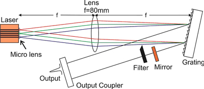
Photonic crystal fibers (PCFs) infiltrated with high-index liquids are promising candidates for manufacturing a variety of tunable optical devices. Since the infiltrated fibres guide by the photonic bandgap effect, spectral filtering is an obvious possibility, but other functionalities can also be envisaged. Infiltration of liquid crystals (LCs) seems particularly interesting, due to the very high temperature sensitivity of these materials. Furthermore, the possibility of orienting the LC anisotropy by external electric fields opens up the possibility of manufacturing devices for active polarization control. In this talk, I will discuss the fundamental waveguiding properties of this class of anisotropic photonic bandgap waveguides, based on theoretical and experimental work recently done at COM-DTU. Furthermore, I will show a number of experimental results demonstrating the potential of the technology with respect to fabrication of optical components.
![]()
Frederik Krebs
Polymerafdelingen Forskningscenter Risø
Plastiksolceller giver mulighed for direkte omdannelse af sol lys til elektrisk energi og består i sin enkelthed af et tyndt plastik lag der er lagt imellem to elektroder. På Risø forskes der i de grundlæggende principper for plastiksolceller samt i fremstillingsme-toder og stabiliteten under belysning. Foredraget vil præsentere den indsats, der ligger på Risø inden for området.
![]()
Martin F. Jensen, Kasper Vestentoft, Leif Højslet Christensen
Centre for Microtechnology and Surface Analysis, The Danish Technological Institute, Gregersensvej 1, DK-2630 Tåstrup, Denmark.
Laser micromachining has been an area of focus at the Danish Technological Institute since 2002. Starting with polymer microsystems and lab-on-a-chip technology, the area has grown to encompass several different laser systems, from standard CO2 lasers to state-of-the-art femtosecond lasers, with applications as diverse as structuring of medical devices and drilling in tools for injection moulding. In this talk we will review the development of our laser micromachining lab, from being primarily research-oriented into an important support lab for Danish Industry. Several examples will be given of applications with industrial relevance and impact. In the talk we will also present an outlook on the future of laser micromachining in industry, as seen from our point of view. We shall also point out a few key areas where academia and industry have mutual interests and could both benefit from a joint effort.
![]()
Joseph Braat, Delft University of Technology,
Delft, The Netherlands.
We discuss the basic trend for data capacity gain in optical storage, viz. the decrease in wavelength and the increase in numerical aperture (NA) of the scanning objective. A new trend is to exceed the limiting NA value of unity by going to so-called solid-immersion scanning lenses. The main part of the talk will be centered on another means towards higher capacity by applying the multiplexing principle (more 'bits' per 'pit'). In this presentation we focus on the introduction of orbital angular momentum to an optical beam that can be detected through-focus by a well-chosen detector arrangement.
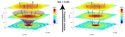
The energy flow through focus for a high-numerical aperture beam (NA=0.85). The arrows indicate the direction of power flow (Poynting vector). Left linear polarization in the entrance pupil of the focusing system. Right The same picture for a right-handed circularly polarized beam of light.
![]()
Towards Cellular and Functional Imaging
Wolfgang Drexler,
Center for Biomedical Engineering and Physics, Christian Doppler Laboratory,
Medical University of Vienna, Austria
Optical coherence tomography (OCT) is an emerging non-invasive, optical medical diagnostic imaging
modality, which enables in vivo cross-sectional tomographic visualization of internal microstructure in
biological systems. Recent developments in ultrabroad bandwidth laser as well as OCT technology enable
three-dimensional ultrahigh resolution OCT with unprecedented axial resolution, approaching resolution
levels of conventional histopathology, enabling optical biopsy of biological tissue.
In addition, extensions of OCT are recently under development that should provide non-invasive depth
resolved functional imaging of the investigated tissue, including extraction of spectroscopic, blood flow
or physiologic tissue information. These extensions of OCT should not only improve image contrast, but
should also enable the differentiation and early detection of pathologies via localized spectroscopic
properties or functional state.
The hypothesis is to provide cellular level resolution visualization of tissue morphology (optical biopsy)
and at the same time localized metabolic and physiologic tissue information in performing a single
volumetric OCT measurement.
![]()
Jes Henningsen, Jan Hald and Jan C. Petersen
Danish Fundamental Metrology, Matematiktorvet B307, 2800 Kgs. Lyngby
jh@dfm.dtu.dk
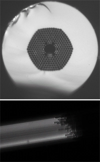
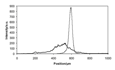
Hollow-core photonic bandgap fibres are well suited for studying the interaction between light and gases, in particular if high light intensity and long interaction length is required. One such case is saturation spectroscopy on weak molecular overtone transitions in the near-infrared spectral region. In conventional spectroscopy the width of an absorption line is determined by the random thermal motion of the molecules through the Doppler effect. In saturation spectroscopy the combination of a strong saturating beam and a weaker counter-propagating beam produces a so-called Lamb dip in the probe absorption when both beams interact with the same velocity class. This is only possible for molecules moving at right angles to both beams, and the Lamb dip thus marks the centre of the Doppler profile. We have used a fibre with a 10 μm core to demonstrate Lamb-dips in acetylene and in carbon-13 substituted hydrogen cyanide. Both molecules are widely used as wavelength references for optical communication in the C-band around 1550 nm, and the use of saturation spectroscopy implies a significant improvement in accuracy of such references.
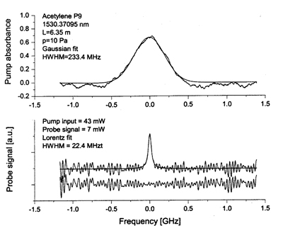
Upper graph shows the Doppler profile of an absorption line in acetylene at 1530.37 nm.
Lower graph shows the suppression of the Doppler effect achieved in a 6.35 m long hollow-core photonic
bandgap fibre.
Acknowledgement
We acknowledge Crystal Fibre A/S for providing the fibre and for sharing their expertise, and the Danish
Research Council for Technology and Production Sciences for financial support under project 26-04-0177
Advanced optical fibre technology: novel concepts and applications.
![]()
Martin Kristensen and Amélie Têtu, University of Aarhus
Department of Physics and Astronomy and Interdisciplinary Nanoscience Center (iNANO),
University of Aarhus, Ny Munkegade, Building 1520,
DK-8000 Århus C, Denmark
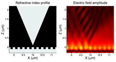
Photonic crystal structures using the photonic bandgap (PBG) effect for horizontal confinement offer
possibilities to engineer integrated optical functions with a packing density approaching that of
integrated electronics. However, both the design and fabrication processes are significantly more demanding
than for conventional integrated optical circuits and the intrinsic propagation loss in these structures is
still higher than for photonic wires having the same dimensions.
The presentation will discuss methods to obtain low loss and large bandwidth of operation for photonic
crystal waveguide components. This includes using a large vertical index step, component design
optimisation using topology optimisation, as illustrated in the figure, and last but not least careful
fabrication including application of high-resolution lithography.
Until recently one of the severe technological limitations of these components was also that they only
worked in one polarisation. However, in many cases it is possible to design the components in such a way
that they allow transmission of both polarisations. This has been confirmed experimentally in a recent
publication [1].
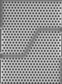
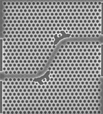
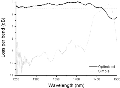
Top left Two simple 60-degree bends. Top right A topology optimised version. Bottom Illustration of the dramatic improvement in performance (from Optics Express 12 (24), 5916-5921 (2004)).
Most of the research was performed in collaboration with DTU under the PIPE project.
[1] A. Tetu, M. Kristensen, L.H. Frandsen, A. Harpøth, P.I Borel, J.S. Jensen and O. Sigmund, 'Broadband topology-optimized photonic crystal components for both TE and TM polarizations', Optics Express 13 (21), 8606-8611 (2005)
![]()
- Combining biology and photonics
Poul Erik Hoiby1, Lars Hagsholm Pedersen1, Jesper Bo Jensen2, Anders Bjarklev2, Theis Peter Hansen2,3, Thomas Nicolaisen3, Jimmi Bak4, Bonni Kryger5, Lars Lindvold6, Lars Lading7
1 Bioneer, DK-2970 Hørsholm, Denmark (www.bioneer.dk), 2 COM-DTU, Technical University of Denmark, DK-2800 Lyngby, Denmark (www.com.dtu.dk), 3 Crystal Fibre A/S, Blokken 84, DK-3460 Birkerød, Denmark (www.crystal-fibre.com), 4 Risø National Laboratory DK-4000 Roskilde, Denmark (www.risoe.com), 5currently at Lumiscence A/S (www.lumiscence.dk), 6 Currently at BFI Optilas A/S, www.bfioptilas.dk, 7 Sensor Technology Center, Gregersensvej 1, Building 6A, DK-2630 Taastrup (www.sensortec.dk)
Poul Erik Hoiby E-mail: peh@bioneer.dk
In recent years the field of biosensors has developed into a fast growing industry. A major sensor-area
is biophotonics involving the fusion of biology and photonics.
From 2001 to 2005 5 Danish companies (Crystal Fibre A/S, Foss A/S, Micro Managed Photons A/S, NUNC A/S,
Optical Verification Components Aps, Sensor Technology Center A/S and 3 research partners (COM at DTU,
Optics and Plasma Physics at Risø National Laboratory, Bioneer A/S) worked together in Center for
Optical Sensors (COS) aiming at developing new ways of analysing biological molecules. COS was focused on
developing:
- planar waveguides
- dual beam FTIR spectroscopical methods
- biosensors made of microstructured fibers and
- Polymer based optical grating sensors.
We will present examples of COS activities but with a focus on optical fibers. Optical fibers with air holes running along the length of the fiber allows for a close proximity of the light guided in the fiber and molecules positioned in the air holes. The penetration of the optical field into the air holes can be significant, making them suitable for sensor applications. This case describes pros and cons concerning the use of microstructured fibers for biosensing
![]()
Peter John Rodrigo, Ivan Perch Nielsen and Jesper Glyckstad,
Optics and Plasma Research Department, Risø National Laboratory, DK-4000 Roskilde, Denmark
We demonstrate the use of multiple optical traps for non-invasive manipulation of various microscopic
objects including microbeads, living yeast cells, and microfabricated silica structures in liquid host
medium. Multiple optical traps are formed using two counterpropagating coaxial light fields, each of which
can be spatially reconfigured in cross-sectional geometry and intensity profile - in a user-interactive
manner or under computer control. Using our tool, three-dimensional user-defined colloidal assemblies of
microbeads have been constructed. Our multiple traps have also been used to facilitate the spatial
arrangement of two different yeast species during a time-lapse growth experiment. A microfabricated
structure can be held and actuated by multiple optical traps by the rounded endings of its appendages. Our
recent experiments show the collective and user-coordinated utility of multiple beams for driving
microstructured objects whose future integration may lead to optically controlled miniaturized
machineries.
Keywords: Optical micro-manipulation, generalized phase contrast (GPC)
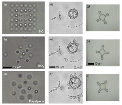
Applications of the GPC-based multiple-beam micromanipulation system. (a) - (c) Various 3D colloidal assemblies of microbeads. (d) - (f) Yeast cell growth experiment. (g) - (i) Optical actuation of a microfabricated structure. See www.ppo.dk for movie-sequences.
![]()
Andrei V. Lavrinenko, Rune S. Jacobsen, Jacob Fage-Pedersen, Lars H. Frandsen,
Beata Zsigri, Christophe Peucheret, and Peter I. Borel.
COM-DTU, NanoDTU, Technical University of Denmark,
Building-345v, DK-2800 Kgs. Lyngby, Denmark
ala@com.dtu.dk
It is believed that so-called slow light, i.e. modes with a group velocity (GV) that is significantly
smaller than the phase velocity in the bulk material, can be used to enhance the light-matter interaction.
Recently experimental support of this statement has been made in several papers. Thus the interest in
utilizing slow light properties is increasing.
Photonic crystal waveguides (PCWs) are known for providing strong nonlinear dispersion together with very
low values of the GV in regions of the dispersion bands flatness. We have made a detailed investigaion of
the GV dispersion in the proximity of the cutoff wavelength of a 2D PCW.
We report on direct numerical calculations and experimental measurements of the GV dispersion in a W1 PCW
by the time-of-flight (ToF) method. The basic concept of measuring the change of the group velocity vs.
wavelength using the ToF is to measure the phase delay of a transmitted, modulated signal for different
wavelengths. The transmitted signal is an envelope function for the intensity of the light, and the phase
velocity of the signal is hence identical to the GV. Taking into account the rather low transmission near
the cutoff wavelength, the modulated light was sent through a short PCW, with a length of 20 μm. The
phase of the envelope function was measured using a network analyzer that both modulates the light and
detects it after the PCW. The calibration measurement for the device was made for a buried waveguide
without a PCW part.
The numerical realization of ToF method was made by finite-difference time-domain (FDTD) modeling. We
launched a TE-polarized impulse from a coupled ridge waveguide into the PCW. The impulse tracking was made
by two detectors placed at the input and output ports of the PCW. By storing fields at all time points we
could restore the dynamics of the impulse propagation through the detectors. By recording at which moments
in time the top of the impulse passes the detectors we calculated time delays, which together with the
known distance between the detectors was used for computing the GV. Both theoretical and experimental
methods revealed a significant decrease of the GV while approaching the mode’s cutoff. We obtained a
reduction of GV down to the values c/230 in experiments and c/500 in simulations, which are the record
values received so far by a ToF method.
![]()
a model system for studying human heart development
Lars Thrane, Risø National Laboratory
The risk of having a newborn child with a cardiac failure is around 0.8%, being the most common birth defect. In Denmark this corresponds to around 500 children each year that are born with a cardiac failure. Basic medical research is carried out in order to understand the mechanisms behind the formation of cardiac failures. The embryonic chick heart is an established model system for studying human heart development, and has been used for many years to study cardiac failures. It has been shown that optical coherence tomography (OCT) is a powerful imaging modality, which can provide new insight in assessing and understanding normal and abnormal cardiac development in the embryonic chick model system. Here, we present very recent results of OCT imaging of the embryonic chick heart using a real-time OCT system with a frame rate of 8 frames per second. The results include a fly-through movie of a beating chick embryo heart, a 3D reconstruction of a day-5 chick heart, and the visualization of the coronary artery and the epicardium.
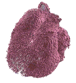
3D OCT scanning of day-5 chick embryo heart.
![]()
Thomas Søndergaard and Sergey I. Bozhevolnyi,
Department of Physics and Nanotechnology, University of Aalborg,
Skjernvej 4C, DK-9220 Aalborg Øst, Denmark
Reply to: thomass@physics.aau.dk
In recent years there has been an increasing interest in optical components based on surface plasmon
polaritons (SPPs) propagating along a planar metal-dielectric interface, or long-range SPPs (LRSPPs)
propagating along a thin metal film. Similar to planar photonic crystals [1], it is also possible to
design optical components based on SPPs by microstructuring the interface, or the surfaces of the metal
film, by periodically arranged metal scatterers in one and two dimensions [2,3].
The loss due to out-of-plane scattering (OUPS) is an important issue for planar optical components. In
this paper a Green’s tensor integral equation method is applied to investigate theoretically how OUPS
losses depend on parameters such as height and spacing of the ridges of a LRSPP grating. We find that the
OUPS is significantly larger for wavelengths below the bandgap compared to wavelengths above the bandgap.
We also find that a design strategy based on small ridge height and long gratings reduces OUPS related to
coupling light into the grating. It is furthermore found that the absorption by the metal structure is
reduced for wavelengths in the bandgap. These issues will be illustrated for a grating designed for
telecommunications wavelengths via calculations of reflection, transmission, out-of-plane scattering and
absorption versus wavelength, as well as field images for selected wavelengths below, in, and above the
bandgap.
[1] J.D. Joannopoulos, R.D. Meade, and J.N. Winn, Photonic crystals, (Princeton University Press,
Princeton, NJ, 1995)
[2] S.I. Bozhevolnyi, A. Boltasseva, T. Søndergaard, T. Nikolajsen and K. Leosson
"Photonic bandgap structures for long-range surface plasmon polaritons", Opt. Comm., 250, 328
(2005).
[3] T. Søndergaard and S.I. Bozhevolnyi, "Theoretical analysis of finite-size surface
plasmon polariton band-gap structures", Phys. Rev. B, 71, 125429 (2005).
![]()
Flemming Olsen
Professor, lic. techn., IPL, DTU
I foråret 1977 ankom den første højeffekt laser til det daværende AMT ved
Danmarks Tekniske Universitet. Det var en 525 w CO2-laser. Det var en stor laser dengang.
Vi var to eksamensprojektstuderende, der stod og ventede spændt på at få fingre i den
laser.
Siden er der gået 28 spændende år, hvor der har været forsket og undervist i
industriel laserteknologi. I alle årene har aktiviteterne været i samarbejde med
industrien.
Temaerne er skiftet i takt med teknologiens globale udvikling og dens indføring i dansk industri.
Først kunne vi ikke skære og svejse tilstrækkeligt store emner, og arbejdet
koncentrerede sig om at imødekomme ønsket om større og hurtigere.
Nu er fokus skiftet: Nu kan det ikke blive småt nok.
I december 1986 stiftedes laser ERFA-gruppen under ATV-SEMAPP. Ønsket var at få en forening i
Danmark, der beskæftigede sig med industriel laserteknologi ud fra industriens synspunkt. I de 19
år, der er gået, har denne ERFA-gruppe arrangeret foredragsdage, erfaringsudveksling og
undervisning for dansk industri. Laserskæring, der er en af de mest udbredte teknologier globalt,
såvel som i Danmark, har i høj grad præget denne forening. I Danmark står i dag
adskillige hundrede CNC-styrede laserskæremaskiner i små og mellemstore virksomheder hvor de
bidrager væsentligt til disse virksomheders eksistens.
Det har for mig været 30 spændende år. Allerede før den første laser
ankom, var jeg som studerende begyndt at forberede mig på modtagelsen af denne laser, så jeg
holder i disse dag 30 års jubilæum med laserteknologi. Teknologiens udvikling har været
utrolig spændende, og det har været spændende at kunne bidrage en lille smule til den.
Indføringen af teknologien i dansk indsutri har været spændende, og jeg har fået
mange gode oplevelser derigennem. Deltagelsen i det internationale netværk af forskere og undervisere
har naturligvis også været utroligt givende.
I dette foredrag vil jeg fortælle high-lights fra disse 30 år samt lidt om, hvilken vej IPL
laseraktiviteter går i dag.
![]()
P. M. Hansen, A. Richardson, K. Berg-Sørensen and L. Oddershede,
Niels Bohr Institute, Blegdamsvej 17, 2100 Copenhagen, Denmark
pmhansen@nbi.dk
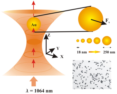
By optical trapping of particles, either naturally occurring lipid granules or artificially inserted gold nanoparticles, we probe the dynamic environment inside a living cell. Our cell of choice is the S. pombe yeast cell. The advantage of using gold nanoparticles rather than the lipid granules is that the gold nanoparticles are well characterized such that they can be used for quantitative measurements. Also, they can be specifically attached to various organelles inside the organism and hence allow for a precise study of the action of that particular organelle. In order to find the correct size of gold nanoparticle for this purpose, we have successfully trapped gold nanoparticles of various sizes, addressing the questions: Which nanoparticles can be optically trapped? Which forces can be exerted on these particles? The gold nanoparticles will be microinjected into living yeast protoplasts, which are cells with their outer cell wall enzymatically stripped off. Regeneration of the protoplasts to viable cells with intact cell wall is successfully done in liquid media. Another potential method to get the gold nanoparticles into the cells is to use ablation methods.To visualize gold nanoparticles inside a living cell is not an easy task, and besides normal brightfield and DIC microscopy, we can use the optical tweezers to prove that the particles are actually inside the cell.
![]()
Det tyske arbejde på at udnytte kerneenergi under 2. verdenskrig
- herunder mødet mellem Heisenberg og Bohr i 1941
Prof. Povl L. Ølgaard
Efter en kort indledning om den fysiske baggrund for interessen for kerneenergi omtales det tyske arbejde på at udvikle en reaktor, som startede allerede i efteråret 1939. Formålet med Heisenbergs besøg hos Bohr i 1941 og forløbet af besøget diskuteres. Et af de store problemer var fremskaffelsen af tilstrækkelige mængder tungt vand. Her udbyggede man produktionsanlægget i Rjukan i det besatte Norge, og problemerne i forbindelse hermed omtales. Også arbejdet med at fremstille beriget uran, hvor tyskerne forsøgte sig med forskellige metoder, diskuteres. Krigens forløb og de tyske fysikeres manglende tro på, at de inden krigens afslutning kunne fremstille et kernevåben, medførte, at det tyske arbejde fra 1942 nedprioriteredes, men fortsattes som forskningsprojekt til krigens slutning. Til slut diskuters hvad det var for faktorer, der gjorde, at det tyske kerneenergiarbejde var så lidet succesfuldt.
![]()
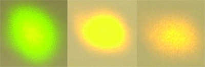
Diodelyskilder til generel belysning
Carsten Dam-Hansen, Birgitte Thestrup og Martin Garmund,
Forskningscenter Risø, Afdelingen for Optik og Plasmaforskning,
Frederiksborgvej 399, 4000 Roskilde
carsten.dam-hansen@risoe.dk | birgitte.thestrup@risoe.dk
martin.garmund@risoe.dk
Lysdioder eller LEDs (Light Emitting Diodes) betegnes som fremtidens lyskilde på grund af deres mange fordele frem for traditionelle lyskilder såsom lang levetid, højt lysudbytte, ingen varme- eller UV-stråling samt kompakte og robuste enheder. Herudover kommer de unikke farvedesign muligheder, idet LED lyskilder kan special designes med hensyn til farvetemperatur og farvegengivelse.
Diode lyskilder.
Pladskrav: et bord til to display kasser ca. 1,2 m x 0.5 m og vægplads til en poster ved siden af.
![]()
Asger C. Krüger, Merete K. Raarup, Martin Kristensen, Jørgen Kjems and Flemming Besenbacher
Interdisciplinary Nanoscience Center (iNANO) and Institute of Physics and Astronomy, University of Aarhus, DK-8000 Aarhus C, Denmark
Conformational switches are vital for the regulation of many cellular processes. In particular the human telomere is believed to contain such a switch, in which opening and closing of a G-quadruplex structure in the telomeric DNA is part of telomere length regulation, which is vital to cell activity. With single-molecule Fluorescence Resonance Energy Transfer (FRET) we are able to detect folding and unfolding of the telomeric G-quadruplex structure in aqueous solution. This allows us to investigate the interactions between the telomeres and telomere binding proteins involved in telomere length regulation, and to study the effect of buffer and salt conditions on the telomeres.
The single-molecule FRET measurements are performed at a new facility that allows for both epi-illumination and Total Internal Reflection (TIR) imaging. The telomeric DNA is tagged with donor and acceptor fluorophores and immobilized to the surface via. biotin streptavidin interactions. The excitation of donor and acceptor molecules is achieved by laser light of 514 nm and 630 nm, matching the absorption spectrum of the donors and acceptors. Fluorescence from donor and acceptors is split into two channels by a wedge mirror and measured by an ultra-sensitive CCD camera. The TIR set-up is based on the prism method, where excitation light is projected onto the sample at a steep angle of incidence, giving rise to an evanescent wave that extends 100 nm into the sample, thus providing less background fluorescence than with ordinary wide-field imaging.
![]()
Brian Bilenberg, Mikkel Schøler, Michael Stenbæk Schmidt, Peter Bøggild, Anders Kristensen
MIC-DTU, Department of Micro and Nanotechnology
and
Peixiong Shi
DANCHIP-DTU
and
Lars Hagedorn Frandsen and Peter Ingo Borel
COM-DTU, Department of Communications, Optics, and Materials, Nano-DTU, Technical University of Denmark (DTU),
Kongens Lyngby, DK-2800 Denmark
http://www.mic.dtu.dk/nil
http://pipe.com.dtu.dk
We present a simple and versatile two-step fabrication scheme for high pattern density silicon stamps for nanoimprint lithography (NIL). The fabrication process relies on electron beam lithography (EBL) followed by reactive ion etching (RIE). We use the negative resist TEBN-1 due to its high resolution, etch resistance, and its high sensitivity. Silicon NIL stamps with isolated lines down to 15 nm and large area homogenous line and dot arrays with a half-pitch down to 30 nm have been fabricated by EBL (JEOL JBX9300FS) in TEBN-1 and subsequent RIE with an optimized SF6/O2/CHF3 based process.
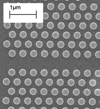
Stamp for fabrication of twodimensional photonic crystal structure. 250 nm half-pitch pillars etched 60 nm into a silicon stamp. The remaining TEBN-1 resist has been removed by oxygen plasma.
![]()
Marina Kasimova, Risø National Laboratory, Denmark
Using fluorescence spectroscopy combined with spectral decomposition analysis we determine the NADH content of actively respiring mitochondria. The reduced coenzyme NADH has a central role in mitochondrial respiratory metabolism. However, reports on the amount of free NADH in mitochondria are sparse and contradictory. While the amount of bound NADH varies, the concentration of free NADH stays relatively unaffected by respiratory state. This suggests that there is a specific mechanism for free NADH homeostasis and that free NADH per se does not play a regulatory role in mitochondrial metabolism. These findings have far-reaching consequences for our interpretation of cellular metabolism.
![]()
Michael Linde Jakobsen, Henning Larsen, Finn Pedersen, Henrik Pedersen, Carsten Dam Hansen, Jørgen Stubager and Steen G. Hanson,
Risø National Laboratory
and
Jørgen Korsgaard, OPDI Technologies, Denmark
A miniaturized optical displacement sensor that can be mounted in a single chip has been built during an
industrial collaboration with the Danish company OPDI Technologies A/S. The system is based on shearing a
speckle pattern arising from a moving surface across a lens array, which here acts as a grating. In some
respects, the function is similar to the function of an eye of a dragonfly. The use of a lens array will in
this setup make it possible not only to get the directional information of the movement but also to
optically establish a dynamic high-pass filtering, thus removing the major part of the low-frequency
speckle noise from the signal.
The system is intended for optical cursor control, and will – compared to existing systems - bring
about a higher number of counts pr. inch and will address a larger range of applications due to the laser
source (VCSEL), the electronic processing and the optics all being imbedded in a single chip.
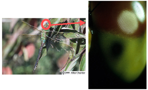
The system is based on shearing a speckle pattern arising from a moving surface across a lens array, which here acts as a grating. In some respects, the function is similar to the function of an eye of a dragonfly.
In short, the optical element, which consists of a single piece of injection-moulded ultem, performs a complex function, which would have been almost impossible, should it have been performed electronically in the ASIC. The master for the lens array part is made by the local nanoplotter (http://www.risoe.dk/ofd/lso/nanoplotter.htm), While the larger lenses and the merging of the two parts is established at another Danish company.
The same technique is applicable for a range of other measurement schemes, including torsional vibrations, linear and angular displacement and in-plane vibrations.
![]()
Johnny Schmidt
J.O. Schmidt, Glahns Alle 17, 2000 Frederiksberg
Hvem opfandt laseren? Man taler om "laseren", som om man mener en ganske bestemt laser. I virkeligheden
er der mange lasere. Der er også mange opfindere af lasere. En videnskabsmand beskriver naturens
fænomener. En opfinder finder på nyttige anvendelser af naturens fænomener. I starten af
det 20. århundrede beskrev Bohr, De Broglie, Einstein og andre, hvordan atomet absorberer og udsender
lys. Ved overgang mellem atomets kvantiserede energitilstande fra en højere til en lavere kan der
produceres elektromagnetisk energi. Einstein (1917) havde forklaret, hvordan stråling kunne stimulere
emission af stråling fra et atom i en højere energitilstand. Forudsætningen var blot, at
den indkomne stråling havde en energi svarende til forskellen mellem den højere og den lavere
energitilstand. To vigtige erkendelser kom dog først senere. Den indkomne og den udsendte
stråling ville være i fase. Og den stimulerede emission ville føre til
forstærkning af den indkomne stråling, hvis antallet af atomer med den højere
energitilstand var stort nok. En sådan forstærkning måtte have nyttige anvendelser. Det
var der flere opfindere der indså.
Townes (US 2,707,235) fik æren for at opfinde en maser. Schawlow og Townes (US 2,929,922) blev anset
for at have opfundet en optisk maser eller en laser, som den senere blev kaldt. Det skulle dog vise sig, at
Gordon Gould var "first-to-invent" i den amerikanske patentlovs forstand. Han var den første, der
tilstrækkeligt tydeligt beskrev lasere med kommercielt vigtige aspekter f.eks. en optisk pumpet laser
og en gaslaser (US 4,053,845; US 4,161,436; US 4,704,583; og US 4,746,201).
Efter 30 års kamp med patentmyndigheder og den amerikanske laserindustri vandt Gordon Gould. Han fik
sine patenter. Det første patent US 4,053,845 fik han i 1977 - 18 år efter indleveringen af
patentansøgningen d. 6. april 1959. Det sidste patent US 4,746,201 fik han i 1988. Det udløb
efter datidens løbetidsregel 17 år efter udstedelsen af patentet d. 24. maj i år -
året hvor Gordon Gould døde 85 år gammel d. 16. september 2005.
Notesbøger har altid været vigtige i amerikanske patentsager, når det skulle
afgøres hvem, der var den første til at gøre en opfindelse. Gordon Goulds notesbog fra
november 1957 skulle vise sig at få afgørende betydning. Vigtigheden af notesbøger
gælder også i dag.
Kendt teknik, patenter på de første lasere, og relevante dele af amerikansk patentlov,
herunder patentability (prior art, novelty, non-obviousness), the specification (enabling written
description, claims, drawings), interference, reissue, reexamination, og specielle emner som antedating
references (conception, diligence, reduction-to-practice) og notebooks vil blive præsenteret.
![]()
Ole Bjarlin Jensen, Peter E. Andersen and Birgitte Thestrup,
Risø National Laboratory, Optics and Plasma Research Department
Frederiksborgvej 3909, DK-4000 Roskilde
ole.jensen@risoe.dk | peter.andersen@risoe.dk
birgitte.thestrup@risoe.dk
Broad area laser diodes and diode laser bars are attractive laser sources due to their small size, high power and high efficiency. Their use is however limited by the poor beam quality in the slow axis. We will present results on the improvement of the beam quality for a segmented broad area laser. The beam quality of the laser is improved by a factor of 23 as compared to the freely running laser.
![]()
1,2A. Purice, 1J. Schou, 3P. Kingshott and 2M. Dinescu
1Department of Optics and Plasma Research, Risø National Laboratory, DK-4000 Roskilde, Denmark, 2National Institute for Laser, Plasma and Radiation Physics, PO Box MG-16 Magurele, 077125 Bucharest, Romania, 3Danish Polymer Centre, Risø National Laboratory, DK-4000, Roskilde, Denmark
Polymer processing and polymer thin film production have been of growing interest in the last few years because of their applications in medicine, electronics, optics and biotechnology. Matrix Assisted Pulsed Laser Evaporation (MAPLE) has been studied and used for deposition of thin polymer films with UV and IR lasers. In this work, we have explored how efficiently thin films of polyethylene glycol (PEG) can be grown from a water ice target with 1% PEG dissolved in water which is one of the most convenient solvents. The film surface was studied by optical and scanning electron microscopy (SEM). Information about the chemical composition of the film was obtained by a well-known method, MALDI, and the deposition rate was measured with a quartz crystal microbalance (QCM). The results were compared with those from the literature for irradiation with UV lasers to identify the best deposition conditions for obtaining high quality thin films.
![]()
- A micro fluidic platform for biochemical sensing
Henrik Schiøtt Sørensen, Risø National Laboratory
When illuminating a micro fluidic channel with a coherent laser, a highly modulated fringe pattern
occurs perpendicular to the channel. The bright and dark spots shift their angular position when changing
the refractive index of the sampled liquid inside the channel. Monitoring this shift is the basis of this
sensor. Performed in fused silica capillary tubes has been able to detect changes in the refractive index
at 10-8 level. Here is presented modelling and platform development of this sensor. The optical
train of the capillary tube has been investigated by a ray-tracing model, which has shown good correlation
with the experimental data, including the possibility to perform absolute measurement of the refractive
index with high accuracy. An analytical solution to Maxwell’s equations has also been developed to
further describe the capillary system, including protein-binding studies on the glass surface. This
analytical model has shown to describe the directly backscattered fringe pattern with higher accuracy. The
interferometric sensor has been under constant development in the last 10 years. One major step is to
change from capillary tubes and into the micro fluidic network scenario.
Normal photolithography processes and following casting of the microstructures usually results in
rectangular shaped micro flow system. Those flow chips has been fabricated in elastomer material (PDMS) and
has shown good experimental results on biochemical sensing, such as DNA-hybridization and protein-protein
interaction. The reproducibility of these measurements depends critically on the flow channel dimensions.
Hence, improvements in performance and system integration are predicted by transferring the well-defined
capillary geometry to a polymer chip-based system with a high degree of accuracy and reproducibility. A
final goal is to perform chip scale interferometry (CSI) with as high sensitivity as capillaries and all
the advantages of micro fluidic advances including mixing of samples. Our channel systems are based on
isotropic etching through narrow entry lines defined by photolithographic procedures.
Photolithography has traditionally been employed for the generation of rectangular or triangular shaped
channels. However, in this study we demonstrate its unconventional combination with isotropic wet etching
in fused quartz and in silicon to form well-defined semicircular channels of cross-sectional dimensions of
100µm. A number of optimizations of the etching mask have been performed for achieving a satisfactory
geometry of the flow system. For the etching in fused quartz a metal mask has been used comprising a thin
Cr layer for adhesion and a thick layer of Au for mechanical stability, using buffered HF as etchant. Etch
channels in silicon were defined by a patterned Si3N4 layer, using a mixture of HF,
nitric acid, and acetic acid as etchant. The etched channels have been characterized by microscopy
performed on PDMS replicas and by 3D profilometric measurements. The structure, a half circle, is
electroplated into a nickel replica that is subsequently used as mold for injection molding. Multiple
thermoplastic flow chips have been fabricated and assembled for chip scale interferometry.
The CSI-sensor has shown detection limits of Dn = 1×10⁻⁵, well in the range of
monitoring biological relevant samples.
![]()
Niels Gregersen, COM-DTU
ngr@com.dtu.dk
When studying a structure with sub-wavelength topography in the SNOM microscope, the tip of a tapered single mode fiber is scanned a few tens of nanometers above the sample. The fiber tip couples the free-space optical field to the propagating fiber mode, allowing a measurement of the near-field. The field-image transfer function describing this coupling is investigated using full 3D vectorial modelling.
![]()
Nina Skivesen, Robert Horvath, Henrik C. Pedersen,
Department of Optics and Plasma Research, Risø National Laboratory, DK-4000 Roskilde, Denmark
nina.skivesen@risoe.dk
Peak-type operation of metal-clad waveguide sensors provides a probing depth into the sample volume of
infinity, unlike conventional waveguide sensors, probing depth ~200 nm. Thus, the deep-probe sensor is
applicable for detection of micron-sized biological objects.
A typical optical waveguide sensor is based upon monitoring the resonance angle at which light is coupled
into the waveguide. Hence, the in-coupled light intensity versus illumination angle gives rise to a
peak-type sensorgram. As opposed to this, the metal-clad waveguide is used in reflection mode, see Fig. 1,
just as the well-known surface-plasmon resonance biosensor. Hence, in this case the sensorgram typically
consists of a dip in reflectance versus illumination angle, giving rise to a dip-type sensorgram, see Fig
2.
What is common for all these conventional biosensor techniques is that the resonance angles of the
sensorgrams are quite far from the cut-off angle at the film-sample interface, which is the main reason for
the limited probing depth. If, however, an ultra-thin layer of high-loss metal (large imaginary part of the
permittivity) is used as a metal cladding, the sensorgram changes completely to a peak-type, in which the
peak angle is exactly identical to the critical angle at the film-sample interface, see Fig 3. This causes
the probing depth of the evanescent field to increase to infinity. Moreover, the sensitivity increases to
unity, which is also approximately 5 times larger than for ordinary waveguide sensors [1]. The high probing
depth for metal-clad waveguides operated in peak-type mode widens the field of application to cover
detection of micron-scale biological objects including bacteria and whole cells.
Thus, metal-clad waveguide sensors facilitates two different operation modes depending on the metal used,
dip-type and peak-type operation which are optimal for different sensing purposes such as refractive index
measurements, detection of micron-scale objects or to measure thin adlayers on the sensor surface. The work
to be presented will focus on application of both types of metal-clad waveguide sensors for specific
detection purposes and will also include experimental results with various metal-clad waveguide
configurations.
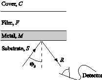
Fig.1: Metal-clad waveguide sensor configuration
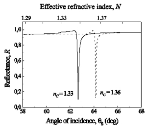
Fig.2: Dip-type sensorgrams of a conventional metal-clad waveguide configuration: glass, 50 nm gold, 300 nm SiO2 and samples nC = 1.33 & nC = 1.36.
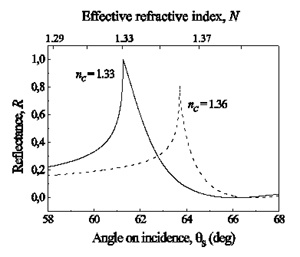
Fig.3: Peak-type metal-clad sensorgrams for a 5 nm titanium-clad waveguide, ε = -3.9 + i12.2: Glass, 5 nm Ti, 250 nm SiO2 and samples nC = 1.33 & nC = 1.36.
1 R. Horvath, L.R. Lindvold and N.B. Larsen, "Reverse-symmetry waveguides: theory and fabrication", Applied Physics B 74, 383 - 393 (2002).
2 N. Skivesen, R. Horvath & H.C. Pedersen, "Optimization of metal-clad waveguide sensors", accepted for publication in Sensors & actuators B.
3 N. Skivesen, R. Horvath & H.C. Pedersen, "Peak-type and dip-type metal-clad waveguide sensing", accepted for publication in Optics Letters.
![]()
Jonas Beermann,
University of Aalborg
Using a second-harmonic far-field scanning optical microscope (SH-SOM) we have previously imaged
randomly distributed gold scatterers deposited on a gold film supporting multiple scattering of surface
plasmon polaritons (SPPs). We observed strongly enhanced localized second-harmonic (SH) spots, exhibiting
wavelength, polarization and scatter density dependence, and very often coinciding with fundamental
harmonic (FH) brighter or darker spots. These effects were attributed to the resonant excitation of SH and
FH eigenmodes existing at nanostructured gold surfaces.
In this work, we investigate periodic arrays of nm-sized gold particles (and groups of gold particles)
deposited on a gold film. Such periodic arrays make it possible to pursue the SH enhancement even further,
and contrary to the measurements on random structures these periodic structures offer the opportunity to
reproduce a particular good configuration to be routinely used at for instance spectroscopy of individual
molecules.
The individual resonances within the particles can be tuned by varying both particle dimensions and
shapes. At the same time resonances for multiple interactions within the grating of particles (scatterers)
can be tuned by varying the grating period. When matching the individual resonance to the grating resonance
strong SH enhancement is expected. Experimental results obtained with periodic arrays using the SH-SOM will
be reported at the conference. We also implement a recently suggested method for quantitative evaluation of
field enhancement.
![]()
Jesper Liltorp Mortensen, Danish Technical University
Efficient generation of continuous-wave (CW) tunable light in the yellow region is reported. The method is based on sum-frequency mixing of a tunable Cr4+:forsterite laser with a Nd:YVO4 laser. A periodically poled lithium niobate crystal was placed intra-cavity in a Nd:YVO4 laser, and the Cr4+:forsterite laser was single-passed through the non-linear media. With this setup it was possible to generate up to 30 milliwatts of yellow light smoothly tunable from 573 to 587 nm
![]()
Peter Kjær Kristensen, University of Aarhus
We apply electric field induced second harmonic (EFISH) to polymer light emitting diodes (PLEDs) and demonstrate the ability to determine the diffusion voltage in PLED devices. The EFISH signal is proportional to the square of the effective field, which is the sum of the diffusion voltage and the applied voltage. By minimizing the EFISH-signal as a function of the applied voltage, the diffusion voltage is determined by measuring the applied voltage that cancels out the diffusion voltage. The PLEDs are fabricated with indium tin oxide (ITO) as the hole injecting contact and two different electron injecting contacts, namely aluminum and calcium. The diffusion voltage originates from the rearranged charges caused by the difference in Fermi levels in the materials in the PLEDs. Different contacts will thus cause different diffusion voltages. We demonstrate here that the EFISH signal is proportional to the square of the effective field in both reverse and forward bias, and discuss the dependence on contact materials.
![]()
Valentyn S. Volkov and Sergey. I. Bozhevolnyi Department of Physics and Nanotechnology, Aalborg University, Skjernvej 4C, DK-9220 Aalborg Øst, Denmark
Peter. I. Borel and Lars. H. Frandsen Research Center COM, Technical University of Denmark, Building 345V, DK-2800 Kgs. Lyngby, Denmark
Martin Kristensen Department of Physics and Astronomy and Interdisciplinary Nanoscience Center(iNANO), University of Aarhus, Ny Munkegade, Building 1520, DK-8000 Århus C, Denmark Department of Physics and Nanotechnology, Aalborg University, Skjernvej 4C, DK-9220 Aalborg Øst, Denmark
volkov@physics.aau.dk
Development of integrated optical components based on planar photonic band gap (PBG) structures, also
called photonic crystals (PCs), has attracted a great deal of attention [1]. The most interesting
applications are related to the possibilities of controlling of light propagation in PCs by introducing
artificial defects and thereby locally disturbing the PBG.
Using a collection SNOM we have performed sub-wavelength characterisation of different PBG components
within their operation bandwidth with tracking of the light propagating in the PC structures. We have
directly mapped the light intensity distribution in a specially designed 50/50 Y-splitter, which is a key
optical component in interferometers and multiplexers. SNOM images have been obtained for the TE- and TM-
polarized light in the wavelength range 1425 – 1630 nm. It was found that the recorded intensity
distributions exhibit highly wavelength (and polarization) dependent intensity variations along the
propagation direction, especially around the fork and bend regions. By comparing the SNOM images recorded
in and after the Y-splitter area, the features of light distribution were analysed. Similar investigations
were also performed for other PCWs components including the PCW with a Z-bend and the wavelength selective
directional coupler.
[1] J. D. Joannopoulos, P. R. Villeneuve, and S. Fan, Nature 386, 143 (1997).
![]()
Nini Pryds, AFM, Jørgen Schou, OPL, and Søren Linderoth, AFM
Risø National Laboratory, DK-4000 Roskilde, Denmark
(AFM, Department of Materials Research; OPL, Department of Optics and Plasma Research)
e-mail: j.schou@risoe.dk
Pulsed laser deposition (PLD) is a unique method for producing thin films of materials of complicated stoichiometry, e.g. metal oxides or metal alloys. Risø National Laboratory has recently established a national facility for making films of large areas. With the present setup uniform films of thickness from a few nanometers up to 1000 nm can be produced on wafers of more than 100 mm of diameter. We have recently also got a grant for a RHEED (Reflected High-Energy Electron Diffraction) instrument which will allow us to produce sandwiches of multilayer films with sharp interfaces at the monolayer level as well as to control the growth rate, film thickness and to determine the lattice spacing.
Plume from a YSZ (yttria-stabilized zirconia) -target irradiated at 248 nm by a KrF-laser in a 0.1-mbar oxygen background gas during deposition of a YSZ-film on a Si wafer. The red triangle above the plume is the hot substrate 85 mm from the target.
![]()
Ilya P. Radko, Sergey I. Bozhevolnyi
Department of Physics and Nanotechnology, Aalborg University, Skjernvej 4C, DK-9220 Aalborg Øst, Denmark
ilya@physics.aau.dk
The concept of transfer function plays an important role in any imaging technique. An amplitude transfer function for collection near-field optical microscopy relates the near-field amplitude and the amplitude of a mode guided in a probe fiber toward a detector. Here we present the results of experimental determination of the transfer function for a scanning near-field optical microscope operating in collection mode and, using reciprocity principle, for that operating in illumination mode. Data for propagating and evanescent plane-wave components are presented and compared with experimental and theoretical results available. We observe that, in general, the transfer functions determined for different probes and light polarizations exhibit rather complicated behavior. However, we find that one can approximate this behavior in the high spatial frequency range corresponding to the evanescent waves by an exponential fall-off associated with notion of an effective detection point situated inside a fiber tip, typically a fraction of the light wavelength away from its extremity.
![]()
Carsten Dam-Hansen, Henrik Pedersen, Jørgen Stubager, Michael Linde Jakobsen, Finn Pedersen, Henning Larsen and Steen G. Hanson
Risø National Laboratory, Optics and Plasma Research Department, 4000 Roskilde
and Jørgen Korsgaard
OPDI Technologies, Denmark
carsten.dam.hansen@risoe.dk
Miniaturized and cheap optical sensors can be facilitated if the optical functions can be integrated into a single element that can be massproduced by injection molding. Here we present a newly developed polymer optical element for an optical sensor to be used in an optical mouse. The element is double sided, one side with three millimetre sized refractive lenses and the other contains three micro optical lens arrays.
Nickel shim for production of microoptical element.
The microoptics side of the element is produced by direct laser writing using Risøs Nanoplotter. Master elements with the designed pitch, size and radii of curvature are produced in photoresist through accurate control over the writing parameters and topographical measurements. A nickel shim is produced by galvano-forming from the master element, and the shim is then used as the one side in the mould cavity. The process steps will be described and comparisons of surface topography measurements of the master, shim and polymer replica will be presented.
![]()
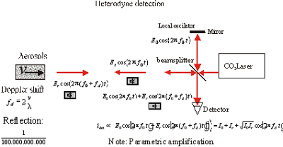
René Skov Hansen
Optics and Plasma Research dept., Risø National Laboratory, Frederiksborgvej 399, DK-4000 Roskilde, Denmark.
e-mail: rene.skov.hansen@risoe.dk
A demonstration system for a laser Doppler anemometer has been developed. The basic principle of the set-up is a Michelson interferometer where the airborne aerosols constitute one of the back-reflecting mirrors. The wind speed along the laser beam is determined from the time varying interference between the back-scattered light and the reference beam from the second arm in the Michelson interferometer. The frequency of the changes of the interference pattern to be detected is determined by the Doppler shift of the back-scattered light.